VOXL 2 Mini Connectors
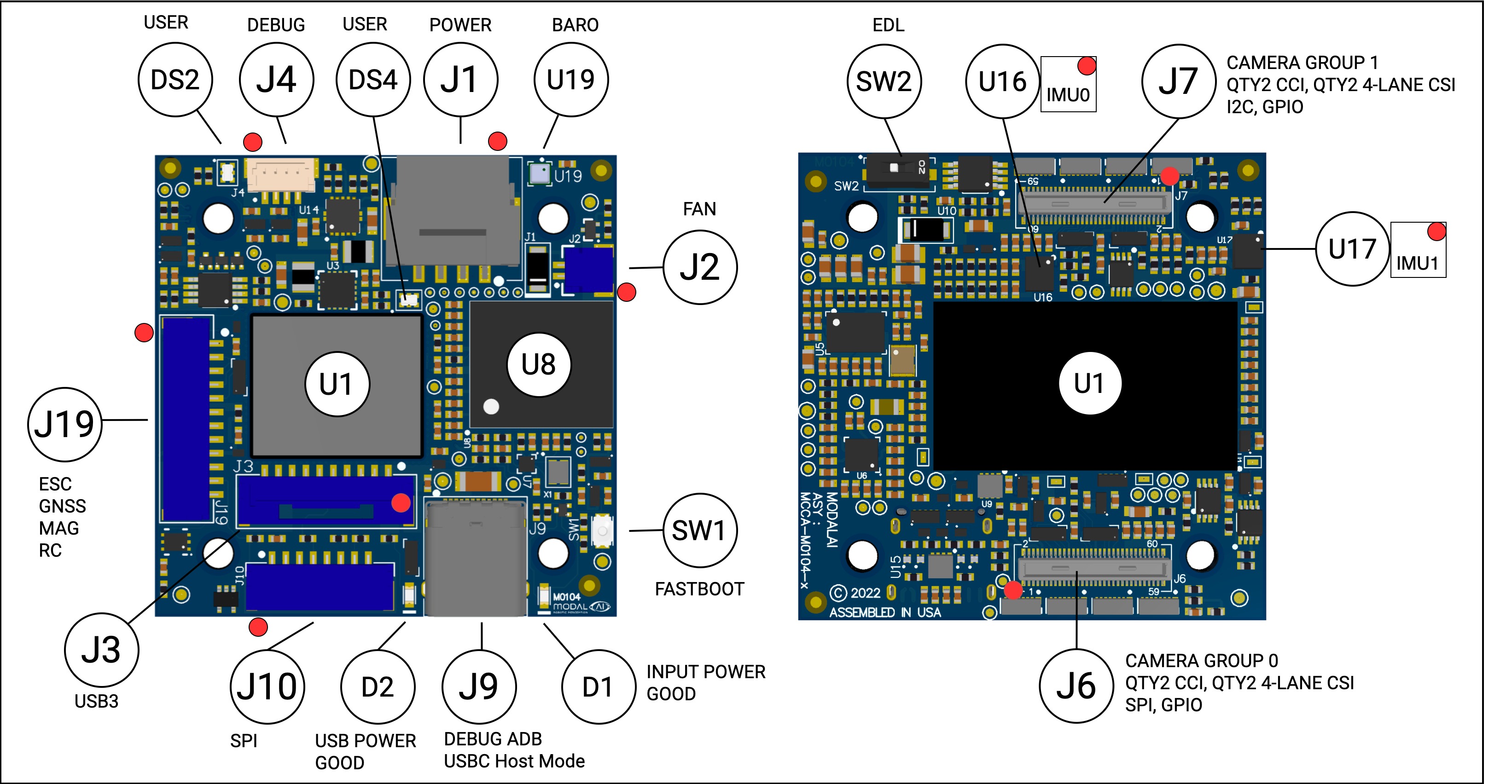
Table of contents
- Summary
- Pinouts
- «««< HEAD
Summary
Below describes the VOXL 2 Mini connectors.
All single ended signals on B2B connectors J6 and J7 are 1.8V CMOS unless explicitly noted. All single ended signals on cable-to-board connectors J10, J19 are 3.3V CMOS unless explicitly noted.
| Connector | Description | MPN (Board Side) | Mating MPN (Board/Cable Side) | Type | Signal Feature Summary |
|---|---|---|---|---|---|
| J1 | Prime Power In, 3.8V | Molex 2059-72-0041 | 2059792041 | Cable Connector, 4-pin R/A | +3.8V main DC power in + GND, I2C@3.8V for power monitors |
| J2 | Fan | SM02B-SRSS-TB(LF)(SN) | SHR-02V-S | Cable Header, 2-pin R/A | 5V DC output for FAN + PWM Controlled FAN-Return (GND) |
| J3 | USB3 | BM10B-GHS-TB(LF)(SN) | GHR-10V-S | Cable Header, 10-pin vertical | |
| J4 | Debug console | BM04B-SRSS-TB(LF)(SN) | SHR-04V-S | Cable Header, 4-pin vertical | Linux debug console enabled in debug kernel builds only |
| J6 | Camera Group 0 | DF40C-60DP-0.4V(51) | DF40C-60DS-0.4V | B2B Plug, 60-pin | Qty-2 4L MIPI CSI ports, CCI and camera control signals, 8 power rails (from 1.05V up to 5V) for cameras and other sensors, dedicated SPI, GPIO |
| J7 | Camera Group 1 | DF40C-60DP-0.4V(51) | DF40C-60DS-0.4V | B2B Plug, 60-pin | Qty-2 4L MIPI CSI ports, CCI and camera control signals, 8 power rails (from 1.05V up to 5V) for cameras and other sensors, dedicated I2c, GPIO |
| J9 | USB-C (ADB) | 12401610E4#2A | USB Type-C | Cable Receptacle, 24-pin R/A | ADB USB-C with OTG/Host mode support (no Display Port) (USB0) |
| J10 | UART/SPI Expansion | SM08B-GHS-TB(LF)(SN) | GHR-08V-S | Cable Header, 8-pin R/A | UART (or SPI with 2 CS_N pins), 32kHz CLK_OUT (resistor option), all 3.3V CMOS signal levels |
| J19 | ESC/GNSS/MAG/RC | SM12B-GHS-TB(LF)(SN) | GHR-12V-S | Cable Header, 12-pin R/A | RC UART@3.3V, ESC UART@3.3V, GNSS UART@3.3V, Magnetometer I2C@3.3V, 5V, 3P3V_RC (SW controllable) |
Pinouts
J1 - Power Connector / I2C Battery Monitoring
Note: for use with ModalAI Power Module V3 in the “-4” config set to 3.8V.
| Pin# | Signal | Notes/Usage |
|---|---|---|
| 1 | VBAT_IN_3P8V | DC from Power Module, 3.8V nominal/fixed or 1S ranges (3.3V to 4.25V) |
| 2 | GND | Power Module Return |
| 3 | I2C_CLK_3P8V | SSC_QUP_1, 3.8V signal levels, Pullups on Power Module |
| 4 | I2C_SDA_3P8V | SSC_QUP_1, 3.8V signal levels, Pullups on Power Module |
J2 - 5VDC Fan Control
| Pin # | Signal Name | Notes |
|---|---|---|
| 1 | VDC_5V_LOCAL | 5V power output ** |
| 2 | FAN RETURN (GND) | Return limited to ~400mA |
J3 USB 3 10-pin
This format is identical to M0090, M0130
| Pin# | Signal | Notes/Usage |
|---|---|---|
| 1 | 5VDC | 5V VBUS power output, 900mA total when VBAT_IN = 3.8V ** |
| 2 | USB1_HS_HUB3_CON_D_N | EMI/ESD filters on-board |
| 3 | USB1_HS_HUB3_CON_D_P | EMI/ESD filters on-board |
| 4 | GND | |
| 5 | USB1_HUB3_SS_RX_N | EMI/ESD filters on-board |
| 6 | USB1_HUB3_SS_RX_P | EMI/ESD filters on-board |
| 7 | GND | |
| 8 | USB1_HUB3_SS_TX_N | EMI/ESD filters on-board |
| 9 | USB1_HUB3_SS_TX_P | EMI/ESD filters on-board |
| 10 | GND |
«««< HEAD
- Note: There is a known HW issue on the USB3 Super-speed TX lines where the AC caps are not included. Please include AC caps on any mating HW, both RX and TX, or your link may be limited to USB2 speeds. We plan to fix this on a future spin of Voxl2 Mini. Our MCBL-00022 host port adapter can be manually modified to insert serial caps on the TX lines using radial components as a work-around if using a COTS USB3 device.
documentation/master
J4 - Serial Debug Port
This format is identical to other ModalAI debug ports
| Pin# | Signal | Notes/Usage |
|---|---|---|
| 1 | VREG_3P3V_LOCAL | 3.3V Power Output * |
| 2 | DEBUG_UART_RX_3P3V | QUP_12 UART Receive (input), 3.3V signal levels |
| 3 | DEBUG_UART_TX_3P3V | QUP_12 UART Transmit (output), 3.3V signal levels |
| 4 | GND |
Camera Group J6, J7
General Pin-out
Generic camera group pinout, please work with ModalAI for any mating designs to gauranteee proper operation
| Pin# | Signal |
|---|---|
| 1 | GND |
| 2 | GND |
| 3 | Lower CCI_I2C_SDA |
| 4 | DVDD 1.2V |
| 5 | Lower CCI_I2C_SCL |
| 6 | DOVDD 1.8V |
| 7 | GND |
| 8 | DVDD 1.05V |
| 9 | Lower CSI_CLK_P |
| 10 | Lower RST_N |
| 11 | Lower CSI_CLK_M |
| 12 | Lower MCLK |
| 13 | Lower CSI_DAT0_P |
| 14 | GND |
| 15 | Lower CSI_DAT0_M |
| 16 | Lower CCI Timer |
| 17 | GND |
| 18 | Upper CCI Timer |
| 19 | Lower CSI_DATA1_P |
| 20 | Upper MCLK |
| 21 | Lower CSI_DATA1_M |
| 22 | AVDD 2.8V |
| 23 | Lower CSI_DATA2_P |
| 24 | GND |
| 25 | Lower CSI_DATA2_M |
| 26 | Upper RST_N, Shared |
| 27 | GND |
| 28 | Upper CCI_I2C_SDA |
| 29 | Lower CSI_DATA3_P |
| 30 | Upper CCI_I2C_SCL |
| 31 | Lower CSI_DATA3_M |
| 32 | Spare MCLK/GPIO |
| 33 | GND |
| 34 | Group SPI MISO (groups 0/1) |
| 35 | Upper CSI_CLK_P |
| 36 | Group SPI MOSI (groups 0/1) |
| 37 | Upper CSI_CLK_M |
| 38 | Group SPI SCLK (groups 0/1) |
| 39 | Upper CSI_DATA0_P |
| 40 | Group SPI CS_N (groups 0/1) |
| 41 | Upper CSI_DATA0_M |
| 42 | VREG_S4A_1P8 |
| 43 | GND |
| 44 | GND |
| 45 | Upper CSI_DATA1_P |
| 46 | VPH_PWR 3.8V |
| 47 | Upper CSI_DATA1_M |
| 48 | VPH_PWR 3.8V |
| 49 | Upper CSI_DATA2_P |
| 50 | GND |
| 51 | Upper CSI_DATA2_M |
| 52 | 3.3V |
| 53 | GND |
| 54 | GND |
| 55 | Upper CSI_DATA3_P |
| 56 | 5V |
| 57 | Upper CSI_DATA3_M |
| 58 | 5V |
| 59 | GND |
| 60 | GND |
J6 - Camera Group 0 Specific Pinout
VOXL 2 Mini supports Camera Group 0 and 1 from the VOXL 2 Camera Configs.
Connector: DF40C-60DP-0.4V(51)
Device Tree:
qcom,cam-sensor0qcom,cam-sensor1
J6 Pin-out
| Pin # | Signal Name | Usage / Notes |
|---|---|---|
| 1 | GND | |
| 2 | GND | |
| 3 | CCI_I2C0_SDA | CAM0_CCI0_SDA, gpio101 |
| 4 | VREG_PM8009_L2_1P2 | DVDD 1.2V |
| 5 | CCI_I2C0_SCL | CAM0_CCI0_SCL, gpio102 |
| 6 | VREG_PM8009_L7_1P8 | CAM0_VIO_1P8, CAM0_VIO_1P8 |
| 7 | GND | |
| 8 | VREG_PM8009_L1_1P05 | CAM0_VDD_1P05, NOTE: current this is ~1.13VDC |
| 9 | CSI0_CLK_CON_P | |
| 10 | GPIO_93_CAM0_RST_N | CAM0_RST_N, gpio93 |
| 11 | CSI0_CLK_CON_N | |
| 12 | GPIO_94_CAM_MCLK0_CON | CAM_MCLK0_CON, gpio94 |
| 13 | CSI0_LANE0_CON_P | LEFT |
| 14 | GND | |
| 15 | CSI0_LANE0_CON_N | LEFT |
| 16 | GPIO_110_CCI_TIMER1 | (unused in version 0) |
| 17 | GND | |
| 18 | GPIO_113_CCI_TIMER4 | CAM_FSYNC_1_OUT, CAM_FSYNC0_IN |
| 19 | CSI0_LANE1_CON_P | RIGHT |
| 20 | CAM_MCLK1_CON | CAM_MCLK1_CON, gpio95 |
| 21 | CSI0_LANE1_CON_N | RIGHT |
| 22 | VREG_PM8009_L5_2P8 | CAM0_AVDD_2P8, CAM1_AVDD_2P8 |
| 23 | CSI0_LANE2_CON_P | |
| 24 | GND | |
| 25 | CSI0_LANE2_CON_N | |
| 26 | GPIO_109_CAM3_RST_N | (shared, CAM3_RST_N) |
| 27 | GND | |
| 28 | CCI_I2C1_SDA | CAM1_CCI1_SDA, CAM4_CCI1_SDA |
| 29 | CSI0_LANE3_CON_P | |
| 30 | CCI_I2C1_SCL | CAM1_CCI1_SCL, CAM4_CCI1_SCL |
| Pin # | Signal Name | Notes |
|---|---|---|
| 31 | CSI0_LANE3_CON_N | |
| 32 | MCLK6_G0_CON | (shared) CAM1_RST_N, gpio100, |
| 33 | GND | |
| 34 | GPIO_28_CAM0_SPI0_MISO | /dev/spidev0.0 |
| 35 | CSI1_CLK_CON_P | |
| 36 | GPIO_29_CAM0_SPI0_MOSI | /dev/spidev0.0 |
| 37 | CSI1_CLK_CON_N | |
| 38 | GPIO_30_CAM0_SPI0_CLK | /dev/spidev0.0 |
| 39 | CSI1_LANE0_CON_P | |
| 40 | GPIO_31_CAM0_SPI0_CS | /dev/spidev0.0 |
| 41 | CSI1_LANE0_CON_N | |
| 42 | VREG_S4A_1P8 | |
| 43 | GND | |
| 44 | GND | |
| 45 | CSI1_LANE1_CON_P | |
| 46 | VPH_PWR | |
| 47 | CSI1_LANE1_CON_N | |
| 48 | VPH_PWR | |
| 49 | CSI1_LANE2_CON_P | |
| 50 | GND | |
| 51 | CSI1_LANE2_CON_N | |
| 52 | VREG_3P3V_LOCAL | |
| 53 | GND | |
| 54 | GND | |
| 55 | CSI1_LANE3_CON_P | |
| 56 | VDC_5V_LOCAL | |
| 57 | CSI1_LANE3_CON_N | |
| 58 | VDC_5V_LOCAL | |
| 59 | GND | |
| 60 | GND |
J7 - Camera Group 1 Specific Pinout
VOXL 2 Mini supports Camera Group 0 and 1 from the VOXL 2 Camera Configs.
Connector: DF40C-60DP-0.4V(51)
Device Tree:
qcom,cam-sensor2qcom,cam-sensor3
J7 Pin-out
| Pin # | Signal Name | Usage / Notes |
|---|---|---|
| 1 | GND | |
| 2 | GND | |
| 3 | CCI_I2C2_SDA | CAM2_CCI1_SDA, gpio105 |
| 4 | VREG_PM8009_L2_1P2 | (M0084, R1 not stuffed, not routed) |
| 5 | CCI_I2C2_SCL | CAM2_CCI1_SCL, gpio106 |
| 6 | VREG_PM8009_L7_1P8 | CAM2_DOVDD_1P8, CAM3_DOVDD_1P8 |
| 7 | GND | |
| 8 | VREG_PM8009_L1_1P05 | (M0084, R2 stuffed) CAM2_VDD_1P05,CAM3_VDD_1P05 (NOTE: current this is ~1.13VDC) |
| 9 | CSI2_CLK_CON_P | |
| 10 | GPIO_92_CAM1_RST_N | RST_LOWER_N, gpio92 |
| 11 | CSI2_CLK_CON_N | |
| 12 | GPIO_96_CAM_MCLK2 | MCLK_LOW, gpio96 |
| 13 | CSI2_LANE0_CON_P | |
| 14 | GND | |
| 15 | CSI2_LANE0_CON_N | |
| 16 | GPIO_111_CCI_TIMER2 | CCI_TIMER_LOWER |
| 17 | GND | |
| 18 | GPIO_114_CCI_ASYNC_IN | CCI_TIMER_UPPER |
| 19 | CSI2_LANE1_CON_P | |
| 20 | GPIO97_CAM_MCLK3_CON | MCLK_UPPER, gpio97 |
| 21 | CSI2_LANE1_CON_N | |
| 22 | VREG_PM8009_L6_2P8 | AVDD_2P8, CAM2_DOVDD_2P8, CAM3_DOVDD_2P8 |
| 23 | CSI2_LANE2_CON_P | |
| 24 | GND | |
| 25 | CSI2_LANE2_CON_N | |
| 26 | GPIO_109_CAM3_RST_N | (shared, RST_UPPER_SHARED_N) |
| 27 | GND | |
| 28 | CCI_I2C3_SDA | CAM3_CCI3_SDA, CAM5_CCI3_SDA, gpio107 |
| 29 | CSI2_LANE3_CON_P | |
| 30 | CCI_I2C3_SCL | CAM3_CCI3_SCL, CAM5_CCI3_SCL, gpio108 |
| Pin # | Signal Name | Notes |
|---|---|---|
| 31 | CSI2_LANE3_CON_N | |
| 32 | MCLK6_G1_CON | (shared) GPIO_MCLK6_SHARED, gpio100 |
| 33 | GND | |
| 34 | GPIO_4_CAM1_SPI1_MISO | GPIO_4, /dev/i2c-4 |
| 35 | CSI3_CLK_CON_P | |
| 36 | GPIO_5_CAM1_SPI1_MOSI | GPIO_5, /dev/i2c4 |
| 37 | CSI3_CLK_CON_N | |
| 38 | GPIO_6_CAM1_SPI1_CLK | GPIO_6, |
| 39 | CSI3_LANE0_CON_P | |
| 40 | GPIO_7_CAM1_SPI1_CS | GPIO_7, |
| 41 | CSI3_LANE0_CON_N | |
| 42 | VREG_S4A_1P8 | |
| 43 | GND | |
| 44 | GND | |
| 45 | CSI3_LANE1_CON_P | |
| 46 | VPH_PWR | |
| 47 | CSI3_LANE1_CON_N | |
| 48 | VPH_PWR | |
| 49 | CSI3_LANE2_CON_P | |
| 50 | GND | |
| 51 | CSI3_LANE2_CON_N | |
| 52 | VREG_3P3V_LOCAL | |
| 53 | GND | |
| 54 | GND | |
| 55 | CSI3_LANE3_CON_P | |
| 56 | VDC_5V_LOCAL | |
| 57 | CSI3_LANE3_CON_N | |
| 58 | VDC_5V_LOCAL | |
| 59 | GND | |
| 60 | GND |
J10 - External SPI
Overview
J10 Pin-out, SPI Mode, Default (GPIO_67 = HIGH)
Available from apps proc as /dev/spidev14.0.
| Pin# | Signal | Notes/Usage |
|---|---|---|
| 1 | VREG_3P3V_LOCAL | 3.3V Power Output * |
| 2 | MISO (Input) | APPS_QUP_14, 3.3V signal levels |
| 3 | MOSI (Output) | APPS_QUP_14, 3.3V signal levels |
| 4 | SCLK (Output) | APPS_QUP_14, 3.3V signal levels |
| 5 | CS0_N (Output) | APPS_QUP_14, 3.3V signal levels |
| 6 | CS1_N/GPIO_46 (Output) | Second SPI CS_N or GPIO |
| 7 | GPIO_64_INT_N (Input) | Interrupt Input, 3.3V signal levels |
| 8 | GND | GND |
J10 Pin-out, UART Mode, (GPIO_67 = LOW)
NOTE: this requires a TrustZone devcfg and kernel update. Contact forum.modalai.com for inquiries.
| Pin# | Signal | Notes/Usage |
|---|---|---|
| 1 | VREG_3P3V_LOCAL | 3.3V Power Output * |
| 2 | GPI_40 (Input) | 3.3V signal levels |
| 3 | GPO_41 (Output) | 3.3V signal levels |
| 4 | UART_TX (Output) | APPS_QUP_14, 3.3V signal levels |
| 5 | UART_RX (Input) | APPS_QUP_14, 3.3V signal levels |
| 6 | GPI_46 (Input) | 3.3V signal levels |
| 7 | GPI_64_INT_N (Input) | Interrupt Input, 3.3V signal levels |
| 8 | GND | GND |
J19 - External Sensors (2x UART/ 2x I2C)
J19 Pin-out
| Pin # | Signal Name | Notes |
|---|---|---|
| 1 | VDC_5V_LOCAL | GNSS/Mag 5V power output, 900mA total when VBAT_IN = 3.8V ** |
| 2 | GNSS TX 3P3V | slpi_proc, SSC_QUP6, 3.3V signal levels |
| 3 | GNSS RX 3P3V | slpi_proc, SSC_QUP6, 3.3V signal levels |
| 4 | MAG SCL 3P3V | slpi_proc, SSC_QUP0, 3.3V signal levels |
| 5 | MAG SDA 3P3V | slpi_proc, SSC_QUP0, 3.3V signal levels |
| 6 | GND | |
| 7 | ESC_UART_TX 3P3V | slpi_proc, SSC_QUP2, 3.3V signal levels |
| 8 | ESC_UART_RX 3P3V | slpi_proc, SSC_QUP2, 3.3V signal levels |
| 9 | VREG_3P3V_RC | RC power *, controllable via GPIO 159 |
| 10 | RC_UART_TX (Output) | slpi_proc, SSC_QUP7, 3.3V signal levels |
| 11 | RC_UART_RX (Input) | slpi_proc, SSC_QUP7, 3.3V signal levels |
| 12 | GND |
SW Summary
All connected to the DSP, and in the factory configuration are used as follows:
QUP0- I2C for external magnetomterQUP2- PX4 communicates to the VOXL ESC through this UART.QUP6- UART for external GNSS (GPS)QUP7- UART for external RC input
Power Input/Output Important Note:
- All power outputs on cable connectors are rated for 1A, however, the system cannot provide 1A simultaneously on all connectors. Contact ModalAI for design assistance.
** VBUS and all 5V power outputs are limited to 900mA TOTAL for all loads (Fan, VBUS, and external GNSS/Mag)