VOXL Connectors
Table of contents
- Board Connections and Pin-out Specifications
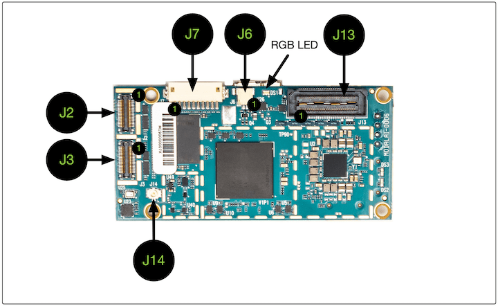
- VOXL Board Top
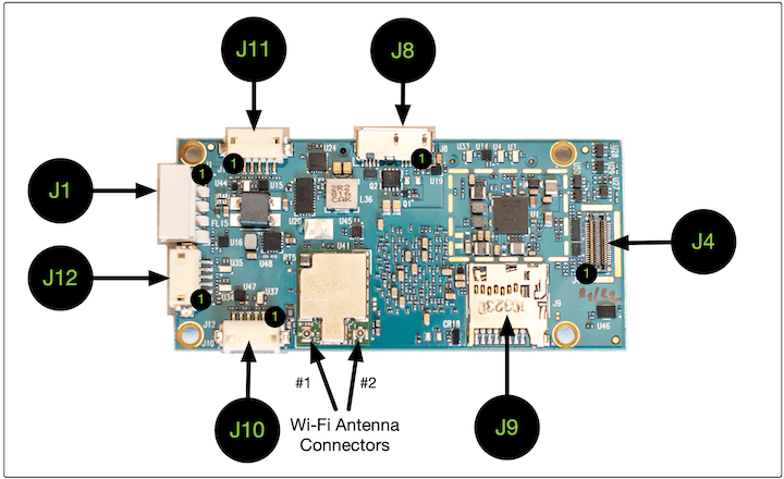
- VOXL Board Bottom
- Connector Pin-outs and Specifications
- J1 5V DC IN, I2C to power cable “APM”
- J2 4k Camera (CSI0)
- J3 Stereo or Time-of-flight Camera (CSI1)
- J4 Tracking/Optic Flow Camera (CSI2)
- J6 Cooling Fan Connector
- J7 BLSP6 (I2C) and BLSP9 (UART / SPI): External GPS/MAG
- J8 USB 3.0 OTG
- J9 Micro-SD Slot
- J10 UART or I2C off-board (external Sonar or IMU sensor)
- J11 BLSP12 off-board (SPEKTRUM)
- J12 BLSP5 off-board (UART ESC)
- J13 Expansion B2B connection
- J14 Integrated GNSS Antenna Connection
- Wi-Fi Antenna Connectors (2)
- RGB LED
- Expansion Board Details
Board Connections and Pin-out Specifications
VOXL Board Top
| Connector | Summary | |
|---|---|---|
| J2 | Hires 4k Image Sensor (CSI0) | Details |
| J3 | Stereo Image Sensor (CSI1) | Details |
| J6 | Cooling Fan Connector | Details |
| J7 | BLSP6 (GPIO) and BLSP9 (UART): External GPS/MAG | Details |
| J13 | Expansion B2B | Details |
| J14 | Integrated GNSS Antenna Connection | Details |
VOXL Board Bottom
| Connector | Summary | |
|---|---|---|
| J1 | 5V DC IN, I2C to power cable “APM” | Details |
| J4 | Tracking/Optic Flow Image Sensor (CSI2) | Details |
| J8 | USB 3.0 OTG | Details |
| J9 | Micro-SD Slot | Details |
| J10 | BLSP7 UART and I2C off-board | Details |
| J11 | BLSP12 UART and I2C off-board (SPEKTRUM) | Details |
| J12 | BLSP5 UART and GPIO off-board (ESC) | Details |
| Wi-Fi | External Wi-Fi antenna connections | Details |
Connector Pin-outs and Specifications
J1 5V DC IN, I2C to power cable “APM”
Pin Configuration
| Pin # | Signal Name | Alt Function |
|---|---|---|
| 1 | 5V DC | |
| 2 | GND | |
| 3 | I2C8_SCL | GPIO 7 |
| 4 | I2C8_SDA | GPIO 6 |
Connector
- Molex Inc, MPN: 22-05-7045
Mating Connector
- 50-37-5043 based cables
Notes
- I2C8 is at 5V CMOS with 10K pull-ups.
- Connect to provided power cable for proper operation and current handling.
J2 4k Camera (CSI0)
Please see Camera Connections page for details on supported configurations.
| J2 Board Connector | Camera (Flex) Mating Connector |
|---|---|
| Panasonic, MPN: AXT336124 | Panasonic MPN: AXT436124 |
Pin-out:
| Pin # | Signal Name | Pin # | Signal Name |
|---|---|---|---|
| 1 | GND | 2 | GND |
| 3 | VREG_L17A_2P8 (AFVDD) | 4 | CAM0_STANDBY_N |
| 5 | CCI_I2C_SDA0 | 6 | VREG_LVS1A_1P8 (DOVDD) |
| 7 | CCI_I2C_SCL0 | 8 | VREG_L3A_1P1 (DVDD) |
| 9 | CAM0_RST0_N | 10 | CAM_MCLK0_BUFF |
| 11 | GND | 12 | GND |
| 13 | MIPI_CSI0_CLK_CONN_P | 14 | CAM_FLASH |
| 15 | MIPI_CSI0_CLK_CONN_M | 16 | CAM_SYNC_0 |
| 17 | MIPI_CSI0_LANE0_CONN_P | 18 | CAM0_MCLK3 |
| 19 | MIPI_CSI0_LANE0_CONN_M | 20 | VREG_L22A_2P8 (AVDD) |
| 21 | GND | 22 | GND |
| 23 | MIPI_CSI0_LANE1_CONN_P | 24 | CAM_RST1_N |
| 25 | MIPI_CSI0_LANE1_CONN_M | 26 | CAM_SYNC_1 |
| 27 | MIPI_CSI0_LANE2_CONN_P | 28 | CCI_I2C_SDA1 |
| 29 | MIPI_CSI0_LANE2_CONN_M | 30 | CCI_I2C_SCL1 |
| 31 | GND | 32 | GND |
| 33 | MIPI_CSI0_LANE3_CONN_P | 34 | VPH_PWR |
| 35 | MIPI_CSI0_LANE3_CONN_M | 36 | GND |
J3 Stereo or Time-of-flight Camera (CSI1)
Please see Camera Connections page for details on supported configurations.
| J3 Board Connector | Camera (Flex) Mating Connector |
|---|---|
| Panasonic MPN: AXT336124 | Panasonic MPN: AXT436124 |
Pin-out:
| Pin # | Signal Name | Pin # | Signal Name |
|---|---|---|---|
| 1 | GND | 2 | GND |
| 3 | VREG_L18A_2P8 (AFVDD) | 4 | CAM1_STANDBY_N |
| 5 | CCI_I2C_SDA0 | 6 | VREG_S4A_1P8 (DOVDD) |
| 7 | CCI_I2C_SCL0 | 8 | VREG_L3A_1P1 (DVDD) |
| 9 | CAM1_RST0_N | 10 | CAM_MCLK1_BUFF |
| 11 | GND | 12 | GND |
| 13 | MIPI_CSI1_CLK_CONN_P | 14 | CAM_FLASH |
| 15 | MIPI_CSI1_CLK_CONN_M | 16 | CAM_SYNC_0 |
| 17 | MIPI_CSI1_LANE0_CONN_P | 18 | CAM1_MCLK3 |
| 19 | MIPI_CSI1_LANE0_CONN_M | 20 | VREG_L23A_2P8 (AVDD) |
| 21 | GND | 22 | GND |
| 23 | MIPI_CSI1_LANE1_CONN_P | 24 | CAM_RST1_N |
| 25 | MIPI_CSI1_LANE1_CONN_M | 26 | CAM_SYNC_1 |
| 27 | MIPI_CSI1_LANE2_CONN_P | 28 | CCI_I2C_SDA1 |
| 29 | MIPI_CSI1_LANE2_CONN_M | 30 | CCI_I2C_SCL1 |
| 31 | GND | 32 | GND |
| 33 | MIPI_CSI1_LANE3_CONN_P | 34 | VPH_PWR |
| 35 | MIPI_CSI1_LANE3_CONN_M | 36 | GND |
J4 Tracking/Optic Flow Camera (CSI2)
Please see Camera Connections page for details on supported configurations.
| J4 Board Connector | Camera (Flex) Mating Connector |
|---|---|
| Panasonic, MPN: AXT336124 | Panasonic MPN: AXT436124 |
Pin-out:
| Pin # | Signal Name | Pin # | Signal Name |
|---|---|---|---|
| 1 | GND | 2 | GND |
| 3 | VREG_L29A_2P8 (AFVDD) | 4 | CAM2_STANDBY_N |
| 5 | CCI_I2C_SDA0 | 6 | VREG_LVS1A_1P8 (DOVDD) |
| 7 | CCI_I2C_SCL0 | 8 | VREG_L3A_1P1 (DVDD) |
| 9 | CAM2_RST0_N | 10 | CAM_MCLK2_BUFF |
| 11 | GND | 12 | GND |
| 13 | MIPI_CSI2_CLK_CONN_P | 14 | CAM_FLASH |
| 15 | MIPI_CSI2_CLK_CONN_M | 16 | CAM_SYNC_0 |
| 17 | MIPI_CSI2_LANE0_CONN_P | 18 | CAM2_MCLK3 |
| 19 | MIPI_CSI2_LANE0_CONN_M | 20 | VREG_L23A_2P8 (AVDD) |
| 21 | GND | 22 | GND |
| 23 | MIPI_CSI2_LANE1_CONN_P | 24 | CAM_RST1_N |
| 25 | MIPI_CSI2_LANE1_CONN_M | 26 | CAM_SYNC_1 |
| 27 | MIPI_CSI2_LANE2_CONN_P | 28 | CCI_I2C_SDA1 |
| 29 | MIPI_CSI2_LANE2_CONN_M | 30 | CCI_I2C_SCL1 |
| 31 | GND | 32 | GND |
| 33 | MIPI_CSI2_LANE3_CONN_P | 34 | VPH_PWR |
| 35 | MIPI_CSI2_LANE3_CONN_M | 36 | GND |
J6 Cooling Fan Connector
Pin Configuration
| Pin # | Signal Name |
|---|---|
| 1 | EXT_FAN_5V |
| 2 | EXT_FAN_RET |
Connector
- J.S.T. Corporation, SM02B-SRSS- TB(LF)(SN)
Mating Connector
VOXL Side:
- J.S.T. Corporation, MPN: SM02B-SRSS- TB(LF)(SN)
Fan Side:
- J.S.T. Corporation
- Connector, MPN: SHR-02V-S
- Connector Contact Pins, MPN: SSH-003T-P0.2-H
Notes
Supported Fan Module:
- DDH Enterprise, Inc, MPN: DDH-2016-013 MCN: 420-59855-0001
J7 BLSP6 (I2C) and BLSP9 (UART / SPI): External GPS/MAG
Pin Configuration
| Pin # | Signal Name | Alt Function |
|---|---|---|
| 1 | VREG_3P3V | |
| 2 | BLSP9_UART_TX_3P3 | GPIO 49 / BLSP9_SPI_MOSI |
| 3 | BLSP9_UART_RX_3P3 | GPIO 50 / BLSP9_SPI_MISO |
| 4 | BLSP6_I2C_SDA_3P3 | GPIO 27 |
| 5 | GND | |
| 6 | BLSP6_I2C_SCL_3P3 | GPIO 28 |
| 7 | BLSP6_AUX2_3P3 | (original docs show GPIO 26, however not functional) |
| 8 | BLSP6_AUX1_3P3 | (original docs show GPIO 25, however not functional) |
| 9 | BLSP9_UART_CTS_N_3P3 | GPIO 51 / BLSP9_SPI_CS_N |
| 10 | BLSP9_UART_RFR_N_3P3 | GPIO 52 / BLSP9_SPI_CLK |
Connector
- HIROSE Electric, MPN: DF13-10P-1.25H.
Mating Connector
VOXL Side:
- HIROSE Electric, MPN: DF13-10P-1.25H.
GPS/MAG Side:
- HIROSE Electric, MPN: DF13- 10S-1.25C.
Notes
Supported GPS Module:
- MCN: 20-CE766-H1 = CCA, H13931V2, SIRFSTARV CREST BOARD REV2
The above uses antenna:
- TAOGLAS LTD, MPN: CGGBP.25.4.A.02
J8 USB 3.0 OTG
Pin Configuration
| Pin # | Signal Name |
|---|---|
| 1 | VBUS |
| 2 | D- |
| 3 | D+ |
| 4 | ID |
| 5 | GND |
| 6 | MICA_SSTX- |
| 7 | MICA_SSTX+ |
| 8 | GND_DRAIN |
| 9 | MICA_SSRX- |
| 10 | MICA_SSRX+ |
Connector
- KYCON, MPN: KMMX- AB10- SMT1SB30
Mating Connector
- Micro A/B Plug
Notes
- Host mode USB 3.0 (e.g. connect a supported USB 3.0 device) requires Micro-A Plug to STD-A in order to get 3.0 SS Functionality. Example cable: Amphenol RUB30-0075 (contact ModalAI for details, available as MCBL-00019-1)
- Host mode USB 2.0 - example cable
J9 Micro-SD Slot
Pin Configuration
| Pin # | Signal Name |
|---|---|
| 1 | DAT2 |
| 2 | CD/DAT3 |
| 3 | CMD |
| 4 | VDD |
| 5 | CLK |
| 6 | VSS (GND) |
| 7 | DAT0 |
| 8 | DAT1 |
Connector
- Molex, MPN: 503398-0891
Mating Connector
- Micro-SD Cards
J10 UART or I2C off-board (external Sonar or IMU sensor)
Pin Configuration
| Pin # | Signal Name | Alt Function |
|---|---|---|
| 1 | VREG_3P3V | |
| 2 | SONAR_UART_TX_3P3 | GPIO 53 |
| 3 | SONAR_UART_RX_3P3 | GPIO 54 |
| 4 | EXT_IMU_I2C_SDA_3P3 | GPIO 55 |
| 5 | GND | |
| 6 | EXT_IMU_I2C_SCL_3P3 | GPIO 56 |
Connector
- HIROSE Electric, MPN: DF13-6P-1.25H(50)
Mating Connector
- DF13-6S-1.25C cable assemblies
Notes
- UART and I2C are at 3.3V CMOS levels.
- Connect TX to target device’s RX, and vice-versa.
- I2C has 10K pull-ups.
J11 BLSP12 off-board (SPEKTRUM)
Pin Configuration
| Pin # | Signal Name | Alt Function |
|---|---|---|
| 1 | VREG_3P3V_SPEKTRUM | |
| 2 | BLSP12_UART_TX_3P3 | GPIO 85 |
| 3 | BLSP12_UART_RX_3P3 | GPIO 86 |
| 4 | BLSP12_I2C_SDA_3P3 | GPIO 87 |
| 5 | GND | |
| 6 | BLSP12_I2C_SCL_3P3 | GPIO 88 |
Connector
- HIROSE Electric, MPN:DF13-6P-1.25H(50)
Mating Connector
- DF13-6S-1.25C cable assemblies
Notes
- UART and I2C are at 3.3V CMOS levels.
- Connect TX to target device’s RX, and vice-versa.
- I2C has 10K pull-ups.
J12 BLSP5 off-board (UART ESC)
Pin Configuration
| Pin # | Signal Name | Alt Function |
|---|---|---|
| 1 | VDCIN_5V | |
| 2 | ESC_UART_TX_5V | GPIO 81 |
| 3 | ESC_UART_RX_5V | GPIO 82 |
| 4 | BLSP5_GPIO_83_5V | GPIO 83 |
| 5 | GND | |
| 6 | BLSP5_GPIO_84_5V | GPIO 84 |
Connector
- HIROSE Electric, MPN: DF13-6P-1.25H(50)
Mating Connector
- DF13-6S-1.25C cable assemblies
Notes
- UART and GPIOs are at 5V CMOS levels
- Connect TX to target device’s RX, and vice-versa.
- GPIO’s are not set for I2C (no pull-ups, push-pull driver).
J13 Expansion B2B connection
Pin Configuration
| Pin # | Signal Name | Pin # | Signal Name |
|---|---|---|---|
| 1 | GND | 2 | VDCIN_5V_CONN |
| 3 | APQ_GPIO_96 | 4 | VDCIN_5V_CONN |
| 5 | APQ_GPIO_95 | 6 | VDCIN_5V_CONN |
| 7 | APQ_GPIO_94 | 8 | USB2_HS_ID |
| 9 | APQ_GPIO_92 | 10 | GND |
| 11 | GND | 12 | USB2_HS_D_M |
| 13 | BLSP11_0_SCL_GPIO61 | 14 | USB2_HS_D_P |
| 15 | BLSP11_1_SDA_GPIO60 | 16 | USB2_HS_VBUS_CONN |
| 17 | BLSP11_2_RX_GPIO59 | 18 | GND |
| 19 | BLSP11_3_TX_GPIO58 | 20 | APQ_GPIO_64 |
| 21 | GND | 22 | APQ_GPIO_127 |
| 23 | BLSP8_0_SCL_GPIO7 | 24 | APQ_GPIO_126 |
| 25 | BLSP8_1_SDA_GPIO6 | 26 | APQ_GPIO_70 |
| 27 | BLSP8_2_RX_GPIO5 | 28 | APQ_GPIO_71 |
| 29 | BLSP8_3_TX_GPIO4 | 30 | APQ_GPIO_72 |
| 31 | GND | 32 | APQ_GPIO_93 |
| 33 | JTAG_TDO | 34 | APQ_GPIO_91 |
| 35 | JTAG_SRST_N | 36 | GND |
| 37 | JTAG_TCK | 38 | APQ_GPIO_106 |
| 39 | JTAG_TDI | 40 | APQ_GPIO_107 |
| 41 | JTAG_TMS | 42 | APQ_GPIO_108 |
| 43 | JTAG_TRST_N | 44 | GND |
| 45 | JTAG_PS_HOLD | 46 | APQ_GPIO_114 |
| 47 | VREG_S4A_1P8 | 48 | APQ_GPIO_104 |
| 49 | PMIC_RESIN_N | 50 | APQ_GPIO_103 |
| 51 | APQ_RESOUT_N | 52 | APQ_GPIO_102 |
| 53 | VREG_3P3V | 54 | APQ_GPIO_101 |
| 55 | KYPDPWR_N | 56 | APQ_GPIO_57 |
| 57 | VPH_PWR | 58 | GND |
| 59 | GND | 60 | PM8996_GPIOC15 |
Connector
- Samtec Inc., MPN: QSH-030-01-L-D-A-K
Mating Connector
VOXL Side:
- Samtec Inc., MPN: QSH-030-01-L-D-A-K
Debug Board Side:
- Samtec Inc, MPN: QTH-030-02- L-D-A-K
Notes
Supported Debug B2B Module:
- Eagle Nest, MCN: 20-H9420-1
- Serial Feather PRO Edition, MCN: 30-H9916-1
More details are available here.
J14 Integrated GNSS Antenna Connection
Pin Configuration
- Center Conductor
Connector
- HIROSE Electric, MPN: U.FL-R- SMT-1(10)
Mating Connector
VOXL Side:
- HIROSE Electric, MPN: U.FL-R- SMT-1(10)
GNSS Antenna Side:
- HIROSE Electric, MPN: U.FL-LP
Notes
Supported Module:
- CABLE ASSY, U.FL TO SMA-F BHD, 1.32 MM COAX MCN: CV90-N5175-A4
- Passive antenna configuration (no DC bias)
Wi-Fi Antenna Connectors (2)
Function
- External Wi-Fi antenna connections
Pin Configuration
- Center Conductor
Connector
- IPEX, MPN: 20449-001E (MHF-4)
Mating Connector
Supported Antennas
Notes
- ANT #1 is for WLAN/BT
- ANT #2 is for WLAN only
RGB LED
Function
- Fixed functionality, momentarily flashes
greenon normal system boot up
Expansion Board Details
The following apply to the expansion board connector J13.
Voltage
Independently, each power rail can provide 1A to circuitry on the B2B mating designs, however, the total current consumed by all power rails should not exceed 1.5A as this ultimately impacts VDCIN_5V_CONN. The signals are listed here:
| Signal | Description and Use |
|---|---|
| GND | Main board ground (DC 0V and signal return path). |
| VDCIN_5V_CONN | This is the same 5V that is present on the Excelsior Flight controller board input power connector (J14) when powered by the provided 5V DC power supply and the APM board. This is primarily used to provide power up to circuitry on the expansion connector’s mating board, up to 1A. |
| VPH_PWR | Main power node input of all the on-board PMIC regulators. This is in the range of 4.15V to 4.25V nominally. This can be used to provide power up to circuitry on the expansion connector’s mating board, up to 1A. |
| VREG_3P3V | Primary 3.3V on the main board. This can be used to provide power up to circuitry on the expansion connector’s mating board, up to 1A. This is useful for voltage translators for the many 1.8V signals. |
| VREG_S4A_1P8 | Primary 1.8V I/O rail on the main board. This can be used to provide power up to circuitry on the expansion connector’s mating board, up to 1A. This is useful for voltage translators for the many 1.8V signals. |
| USB2_HS_VBUS_CONN | USB Port 2 host power. The main board provides a 500mA power switch from VDCIN_5V to provide host-mode support to USB 2.0 peripherals. This is most commonly used to provide the 5V to a USB2.0 HOST connector (Type A) on any mating circuit board. |
USB 2.0
A standard USB 2.0 host port is available on the debug connector. A peripheral can be hard-wired to this port (hub or WLAN application) or a USB compliant Type-A connector can be made available on any mating design for other peripheral types. The signals are listed here:
| Signal | Description and Use |
|---|---|
| USB2_HS_VBUS_CONN | USB Port 2 host power. The main board provides a 500mA power switch from VDCIN_5V to provide host-mode support to USB 2.0 peripherals. |
| USB2_HS_D_P | USB high-speed 2 data – plus |
| USB2_HS_D_M | USB high-speed 2 data – minus |
| USB2_HS_ID | USB-OTG ID pin. This signal is grounded on the main board through a 0- ohm resistor. This is provided only for the application where a Type-A/B (OTG) connector is provided and the ID pin is required to identify the port as a HOST. |
BLSP Signals
Two complete BLSP ports are available on the debug connector. Software, with certain trust-zone limitations, has the ability to configure these ports as a 4-wire UART, 2-wire UART + I2C, I2C + 2 GPIO, SPI, or as four GPIOs. All signals are 1.8V CMOS, and when configured as digital outputs, the drive strength can be set between 2mA – 16mA in 2mA steps. The signals are listed here:
It is advised not to change the configuration of BLSP8 2-wire UART as this is configured as the debug console by default.
| Signal | Description and Use |
|---|---|
| BLSP11_0_SCL_GPIO61 | BLSP port 11, bit 0. RFR when configured for 4-wire UART, SCL when configured as I2C, SPI_CLK when configured as SPI, or GPIO84 when set as GPIO. |
| BLSP11_1_SDA_GPIO60 | BLSP port 11, bit 1. CTS when configured for 4-wire UART, SDA when configured as I2C, SPI_CS_N when configured as SPI, or GPIO83 when set as GPIO. |
| BLSP11_2_RX_GPIO59 | BLSP port 11, bit 2. UART_RX (input) when configured as UART, SPI_MISO when configured as SPI, or GPIO82 when set as GPIO. |
| BLSP11_3_TX_GPIO58 | BLSP port 11, bit 3. UART_TX (output) when configured as UART, SPI_MOSI when configured as SPI, or GPIO81 when set as GPIO. |
| BLSP8_0_SCL_GPIO7 | BLSP port 12, bit 0. RFR when configured for 4-wire UART, SCL when configured as I2C, SPI_CLK when configured as SPI, or GPIO88 when set as GPIO. |
| BLSP8_1_SDA_GPIO6 | BLSP port 12, bit 1. CTS when configured for 4-wire UART, SDA when configured as I2C, SPI_CS_N when configured as SPI, or GPIO87 when set as GPIO. |
| BLSP8_2_RX_GPIO5 | BLSP port 12, bit 2. UART_RX (input) when configured as UART, SPI_MISO when configured as SPI, or GPIO86 when set as GPIO. Note: This is the default debug serial console RX pin |
| BLSP8_3_TX_GPIO4 | BLSP port 12, bit 3. UART_TX (output) when configured as UART, SPI_MOSI when configured as SPI, or GPIO85 when set as GPIO. Note: This is the default debug serial console TX pin. |
Configuration and JTAG Signals
Several configuration and JTAG signals are available on the debug connector. These signals are critical to proper boot-up and system operation, and as such, the end user is advised to not use these signals in any capacity unless they are very securely aware of the boot modes and processes of the VOXL chipset architecture, or with JTAG. Failure to do so could result in a bricked board. The signals are here:
| Signal | Description and Use |
|---|---|
| APQ_GPIO_114 | Advised to ignore signal on any external mating designs. |
| APQ_GPIO_104 | Advised to ignore signal on any external mating designs. |
| APQ_GPIO_103 | Advised to ignore signal on any external mating designs. |
| APQ_GPIO_102 | Advised to ignore signal on any external mating designs. |
| APQ_GPIO_101 | Watchdog disable boot control. Connect to VREG_S3A via 10k-Ohm resistor to disable the watchdog. |
| APQ_GPIO_57 | FORCE_USB_BOOT signal. Connect to VREG_S3A via 10k-Ohm resistor to have the boot loader ignore the programmed image and enter “QDOWNLOAD Mode” to re-image a bricked board. Remove pull-up connection when completed. |
| JTAG_SRST_N | Advised to ignore signal on any external mating designs. |
| JTAG_TCK | Advised to ignore signal on any external mating designs. |
| JTAG_TDI | Advised to ignore signal on any external mating designs. |
| JTAG_TDO | Advised to ignore signal on any external mating designs. |
| JTAG_TMS | Advised to ignore signal on any external mating designs. |
| JTAG_TRST_N | Advised to ignore signal on any external mating designs. |
| JTAG_PS_HOLD | Advised to ignore signal on any external mating designs. |
| PMIC_RESIN_N | PMIC GPIO2 for Reset. Advised to ignore signal on any external mating designs. |
| APQ_RESOUT_N | Advised to ignore signal on any external mating designs. |
| KYPDPWR_N | Advised to ignore signal on any external mating designs. |
Using Configuration GPIOs
As mentioned above, several APQ_GPIOs are reserved for configuration purposes and advised to ignore. However, if these signals must be used, there is a way to utilize them with some added isolation circuitry.
Upon boot up, the applications processor is brought into the correct mode by settings on the Excelsior Flight main board. This boot mode is determined by pin strapping of the boot mode signals upon reset; GPIO_103, and GPIO_[112:116]. After reset, these signals can be reclaimed for general purpose, but it is imperative to keep them tri-stated prior to reset to not interfere with the settings on the Excelsior Flight main board or the applications processor can fail to boot, or boot into an unknown state.
The most effective way to reclaim these signals is to use a bidirectional signal translator with auto-direction sensing and signal isolation with an active high enable pin. This will allow the user to not only voltage translate to the desired level they need, but also allows for either direction usage.
An example schematic of how this can be achieved is shown here:
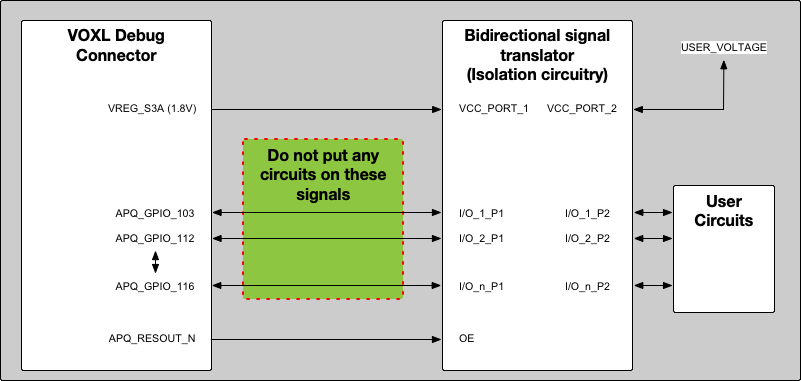
If the exact circuit is not followed, here are the key things to note:
- The translator MUST tri-state the PORT_1 side I/O’s if either VCC_PORT_1 or OE is LOW/GND.
- APQ_RESOUT_N going HIGH is the indicator of when the signals are no longer being sampled for boot mode configuration.
- Be sure the translator can accept 1.8V on VCC_PORT_1, and OE input is referenced to VCC_PORT_1.
- If the direction is known ahead of time, other devices can be used to achieve the desired purpose, such as discrete FETs, but ensure they are logic-level and can operate at VGS of 1V-1.8V.
- DO NOT place any shunt resistors, capacitors, or other circuit elements in-between the GPIOs from the debug connector to the isolation circuits.
- ESD protection is already provided on the Excelsior Flight main board.