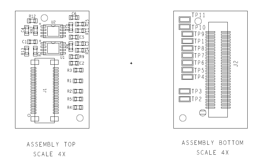
Connects “Lower Group” signals (CSI, Timers, Resets, etc) of either J6, J7, or J8 60-pin DF40 to a Voxl format 36-pin AXT connector. Refer to Voxl2 datasheets for more description on a camera “group”
Pin Out VOXL2-side, J2
Pin
Net
Notes/Usage
1
GND
2
GND
3
Lower CCI_I2C_SDA
Available on J1
4
DVDD 1.2V
Not default, R option
5
Lower CCI_I2C_SCL
Available on J1
6
DOVDD 1.8V
Available on J1
7
GND
8
DVDD 1.05V
Available on J1
9
Lower CSI_CLK_P
Available on J1
10
Lower RST_N
Available on J1
11
Lower CSI_CLK_M
Available on J1
12
Lower MCLK
Available on J1
13
Lower CSI_DAT0_P
Available on J1
14
GND
15
Lower CSI_DAT0_M
Available on J1
16
Lower CCI Timer
Test Point TP2 Only
17
GND
18
Upper CCI Timer
Test Point TP3 and Both Syncs on J1
19
Lower CSI_DATA1_P
Available on J1
20
Upper MCLK
Available on J1
21
Lower CSI_DATA1_M
Available on J1
22
AVDD 2.8V
Available on J1
23
Lower CSI_DATA2_P
Available on J1
24
GND
25
Lower CSI_DATA2_M
Available on J1
26
Upper RST_N, Shared
Available on J1 as CAM_RST_STBY_N
27
GND
28
Upper CCI_I2C_SDA
Available on J1
29
Lower CSI_DATA3_P
Available on J1
30
Upper CCI_I2C_SCL
Available on J1
31
Lower CSI_DATA3_M
Available on J1
32
Spare MCLK/GPIO
Test Point TP4 Only
33
GND
34
Group SPI MISO
Test Point TP5 Only
35
Upper CSI_CLK_P
Not Available/Routed
36
Group SPI MOSI
Test Point TP6 Only
37
Upper CSI_CLK_M
Not Available/Routed
38
Group SPI SCLK
Test Point TP7 Only
39
Upper CSI_DATA0_P
Not Available/Routed
40
Group SPI CS_N
Test Point TP8 Only
41
Upper CSI_DATA0_M
Not Available/Routed
42
VREG_S4A_1P8
Test Point TP1 Only
43
GND
44
GND
45
Upper CSI_DATA1_P
Not Available/Routed
46
VPH_PWR 3.8V
Available on J1
47
Upper CSI_DATA1_M
Not Available/Routed
48
VPH_PWR 3.8V
Available on J1
49
Upper CSI_DATA2_P
Not Available/Routed
50
GND
51
Upper CSI_DATA2_M
Not Available/Routed
52
3.3V
Test Point TP9 only
53
GND
54
GND
55
Upper CSI_DATA3_P
Not Available/Routed
56
5V
Test Point TP10 only
57
Upper CSI_DATA3_M
Not Available/Routed
58
5V
Test Point TP10 only
59
GND
60
GND
Pin Out Mating-side (Voxl format), J1
Pin
Net
Notes/Usage
1
DGND
2
DGND
3
AFVDD
Normally Unused, 2.8V
4
CAM_RST_STBY_N
Normally Unused, power down signal
5
CCI_I2C_SDA0
CCI I2C Bus, SDA
6
1P8_VDDIO
1.8V VDDIO (VREG_S4A or switched VREG_S4A)
7
CCI_I2C_SCL0
CCI I2C Bus, SCL
8
VREG_DVDD
1.1V or 1.2V DVDD
9
CAM_RST0_N
Sensor Reset Control, 0
10
CAM_MCLKx_BUFF
MCLK, Buffered from Voxl2, 1.8V
11
DGND
12
DGND
13
MIPI_CSI_CLK_CONN_P
MIPI CSI High Speed Diff Pair, CLK_P
14
CAM_FLASH
Sensor Sideband Control, Normally Unused
15
MIPI_CSI_CLK_CONN_M
MIPI CSI High Speed Diff Pair, CLK_M
16
CAM_SYNC_0
Sensor Sync Signal, Shorted to SYNC_1 if using M0010
17
MIPI_CSI_LANE0_CONN_P
MIPI CSI High Speed Diff Pair, Data Lane 0_P
18
CAM_MCLK1
Second MCLK, Buffered from Voxl, 1.8V.
19
MIPI_CSI_LANE0_CONN_M
MIPI CSI High Speed Diff Pair, Data Lane 0_M
20
CAM_AVDD_2P8
Sensor 2.8V AVDD
21
DGND
22
DGND
23
MIPI_CSI_LANE1_CONN_P
MIPI CSI High Speed Diff Pair, Data Lane 1_P
24
CAM_RST1_N
Sensor Reset Control, 1
25
MIPI_CSI_LANE1_CONN_M
MIPI CSI High Speed Diff Pair, Data Lane 1_M
26
CAM_SYNC_1
Sensor Sync Signal, Shorted to SYNC_0 if using M0010